


| Place of Origin: | China |
|---|---|
| Brand Name: | WITGAIN PCB |
| Certification: | UL |
| Model Number: | Heavy Copper PCB0002 |
| Minimum Order Quantity: | 1 pcs/lot |
| Price: | negotiable |
| Packaging Details: | Vacuum bubble bag packaging |
| Delivery Time: | 20 days |
| Payment Terms: | T/T |
| Supply Ability: | 100k pcs/month |
| Place Of Origin:: | Guangdong China | Material:: | FR4 TG>170 |
|---|---|---|---|
| No Of Layers:: | 2 Layers | Solder Mask Colour:: | Green |
| Surface Technics:: | HASL Lead Free | Copper Thickness: | 3/3OZ |
| High Light: | Power Supply Hdi Circuit Boards,FR4 hdi circuit boards,3 oz copper pcb |
||
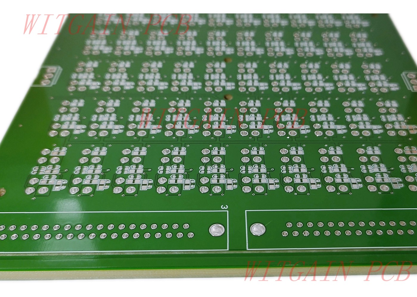
Power Supply PCB FR4 Substrate PCB 2 Layer Heavy Copper 3/3OZ
Main Features:
1 PCB finished thickness to be 3.5mm tolerance +/-10%.
2 Finished copper shoule be at least 3OZ/105um on each layer.
3 Surface treatment on exposed copper pad is HASL lead free.
4 Solder mask color should be green and legend ink color should be white.
5 Power supply main boards.
6 Acceptance standards: IPC-6012 Class3.
7 Rohs and Reach compliant.
Our Product Categories:
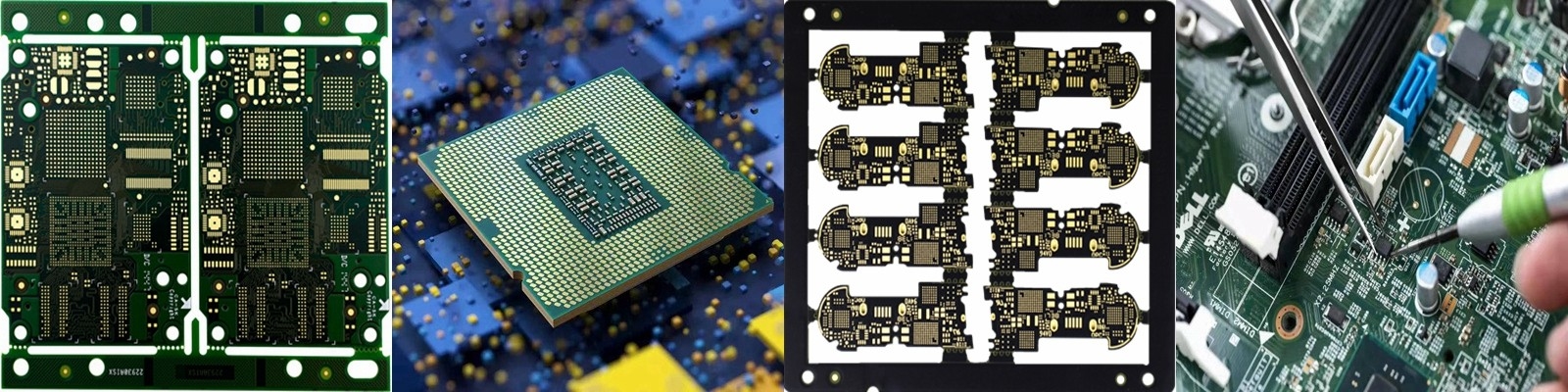
1 FR4 substrate PCB : 2 Layer Printed Circuit Board, 4 Layer PCB, 6 Layer PCB, 8 Layer PCB, 10 Layer PCB, 12 Layer PCB, 14 Layer PCB, 16 Layer PCB, 18 Layer PCB, 20 Layer PCB, 22 Layer PCB, 24 Layer PCB, HDI PCB, High frequency PCB.
2 Aluminum Substrate pcb: 1 Layer Aluminum PCB, 2 Layer Aluminum PCB, 4 Layer Aluminum PCB.
3 Flexible PCB: 1 Layer FPC, 2 Layer FPC, 4 Layer FPC, 6 Layer FPC
4 Rigid-Flex PCB: 2 Layer Rigid-Flex PCB, 4 Layer Rigid-Flex PCB, 6 Layer Rigid-Flex pcb, 8 Layer Rigid-Flex PCB, 10 Layer Rigid-Flex pcb
5 Ceramic substrate pcb: single Layer Ceramic pcb, 2 layer ceramic pcb
FAQ:
Q1: What is peelable solder mask? When is it used? WHat are its advantages and disadvantages?
A1: A Peelable solder mask is a type of solder mask that can be peeled off the surface of a printed circuit board. This type of solder mask is used to protect specific areas of a PCB during reflow soldering, wave soldering, or surface finish process. It is applied over the pads or plated through holes prior to the PCB assembly process and prevents the accumulation of excess solder on empty pads during the soldering process. It also protects gold plated contacts which can dissolve in molten solder. Peelable solder mask is easier to remove than regular solder masks.
Peelable solder masks are also used in selective surface finish processes such as soft gold PCB surface finish or Hard gold PCB surface finish. This type of solder mask ensures that the correct finish is only applied to the desired areas of the PCB. The surface finish is a coating on the bare copper area of the PCB to provide a solderable surface and to protect the exposed copper circuitry.
A peelable solder mask is also necessary for the parts that will be manually installed after the automated assembly process.
Peelable solder masks are usually applied by screen-printing and are removed after processing at the contracted PCB assembly house. The PCB fabricator can apply the mask in any design or shape on one or several sections per side at a time.


