


| Place of Origin: | China |
|---|---|
| Brand Name: | WITGAIN PCB |
| Certification: | UL |
| Model Number: | PCB000382 |
| Minimum Order Quantity: | 1pcs/lot |
| Price: | negotiable |
| Packaging Details: | Vacuum package in bubble wrap |
| Delivery Time: | 20 days |
| Payment Terms: | T/T |
| Supply Ability: | 100kpcs/Month |
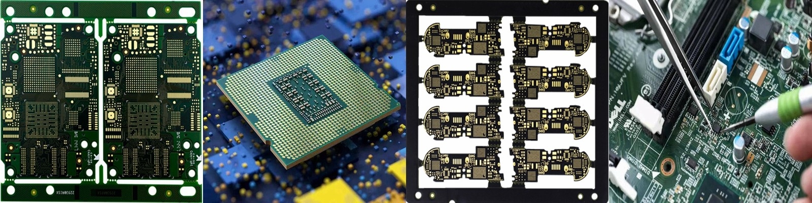
| Layer Count: | 8 Layer | Surface Treatment: | Immersion Gold 3U' |
|---|---|---|---|
| Min BGA PAD: | 12 MIL | Material: | FR4 TG170 |
| Lead Time: | 20 Days | Finished Thickness: | 1.6 MM |
| High Light: | 12 MIL Printed Circuit Boards,OEM Printed Circuit Boards,UL PCB 1.6 MM |
||
Printed Circuit Boards 8 Layer PCB 1.6 MM Finished Board Thickness
Specifications:
1 All dimensions are in MM.
2 Fabricate per IPC-6012A Class2.
3 Materials:
3.1 Dielectric: FR4 Per IPC or equivalent
3.2 Min Tg: 150DEG
3.3 Copper: As per stack up
3.4 UL Rating: 94V0 Minimum
4 Surface finish: ENIG
5 Solder mask material should meet all requirement of the IPC-SM-840E and shall be green in color and applied over bare copper. Vendor may edit solder mask and paste mask as needed.
6 Editing of existing copper layers shall require customer approval.
7 Silkscreen legend to be applied per layer stackup using white non-conductitive epoxy ink.
8 100% continuity testing using database netlist shall be performed.Vendor to identify test passed in secondary side.
9 Vendor to mark date code and logo in legend secondary side.
10 Bow and twist shall not exceed 1.0% of longest side.
11 Vendor to provide panel drawing for customer approval before production
Packing Specifications:
1 One vacuum pcb package should not be over 25 panels based on panel size.
2 The vacuum pcb package sealed must be free to tear, hole or any defects that may cause leakage.
3 The pcb package must be suitable to ensure effective vacuum sealing.
4 Every package must have desiccant and humidity indicator card on the inside of vacuum package.
5 Humidity indicator card target less than 10%.
FQA:
Q1: What is HDI PCB?
A1: HDI is the abbreviation of high density interconnector. Generally, there are blind and buried holes in HDI PCB. Due to the space limits, some product need to very small size pcb. HDI pcb was generated to save space and increase interconnectors.


