


| Place of Origin: | China |
|---|---|
| Brand Name: | WITGAIN PCB |
| Certification: | UL |
| Model Number: | PCB000384 |
| Minimum Order Quantity: | 1pcs/lot |
| Price: | negotiable |
| Packaging Details: | Vacuum package in bubble wrap |
| Delivery Time: | 20 days |
| Payment Terms: | T/T |
| Supply Ability: | 100kpcs/Month |
| Layer Count: | 4 Layer | Surface Treatment: | Immersion Gold 2U' |
|---|---|---|---|
| Application Area: | Vehicle Data Recorder | Material: | FR4 TG150 |
| Impedance Control: | 100 Ohm | Finished Thickness: | 1.2 MM |
| High Light: | Solder Mask Printed Circuit Boards,UL Printed Circuit Boards 4 Layer,FR4 TG150 4 Layer PCB |
||
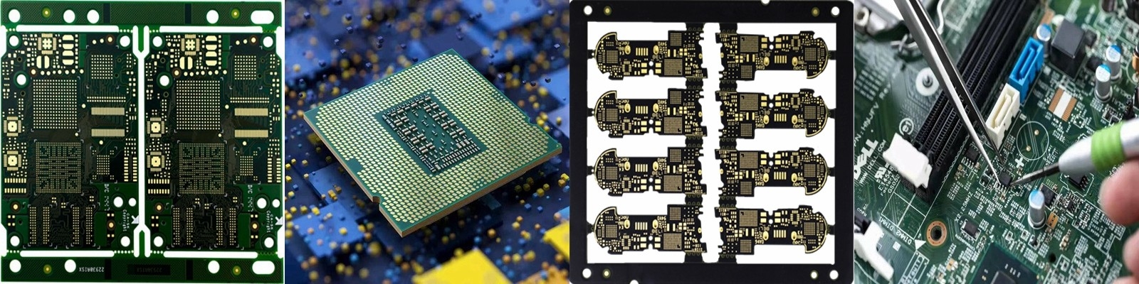
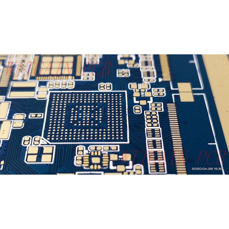
Printed Circuit Boards 4 Layer PCB In Blue Solder Mask
Specifications:
1. Board Laminate:
Board layers 4 layer see layer stackup
Board material laminate should be 0.031inch +/-10%
Finished glass epoxy laminate, type nema grade or equivalent
Outer layer to be 0.5OZ Copper clad
Construction should meet class 94v-0
Layer construction alignment max: +-0.05mm
2. Holes:
Copper plate through all holes with a minimum wall thickness of 0.0254mm
Register tolerance : +-0.015mm
All holes must be drilled +-0.051mm with respect to center of drilled pad
| Delivery Acceptance Requirements: | |
| Test | All boards are tested in accordance with IPC-9252A |
| Working Gerber | Paste layers must be provided on working gerbers. |
| If Paste layer is missing, alert us in EQ. | |
| Fab File | Check original customer Fab file if provided. |
| If there is a conflict between customer FAB and this | |
| document, please ask in your EQ questions. | |
| Approvals | Send working gerber and EQ together. |
| RoHS & REACH | All materials must be RoHS & REACH compliant. |
| All processes must be RoHS & REACH compliant. | |
| Documents | Send PDF copy of all test, measurement, conformance |
| and certificates. No paper or core sample needed. |
FQA:
Q1: What is HDI PCB?
A1: HDI is the abbreviation of high density interconnector. Generally, there are blind and buried holes in HDI PCB. Due to the space limits, some product need to very small size pcb. HDI pcb was generated to save space and increase interconnectors.


