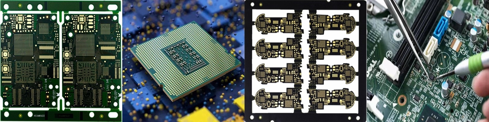
Power Supply PCB 6 Layer Heavy Copper 4 OZ On Each Layer
PCB Specifications:
1. Unless otherwise specified, dimensions on this drawing and gerber data are expressed in mils. Tolerances on this drawing and gerber data when converted to inches are: X.XX +/- 0.01
X.XXX +/- 0.005
Board Cross Section Requirements:
Outer Layer Copper Thickness: +20% / -10%
Inner Layer Copper Thickness: +/- 10%
Overall Board Thickness: +/- 10% Absolute Minimum dielectric spacing shall be 0.00354 in. for 1500V (see Dielectric strength Note 4). Dielectric Spacings: +/- 10%
Angles +/- 2 Degrees Board Feature Requirements:
Unspecified radii: 0.047
Hole to hole: +/- 0.003
PTH diameter: +/- 0.003
NPTH diameter: +/- 0.002
- WORKMANSHIP SPECIFICATION: Class III per latest issue of IPC-6012, IPC-600, and IPC-6011 latest issue, unless otherwise specified. Annular ring to be 1 mil minimum. Via pads may be tear-dropped to meet the annular ring requirement.
Soldermask shall meet IPC-600 Class II thickness requirements.
- Cross section detail specifies expected nominal thicknesses in mils for materials used in board stackup. Two sheet minimum B-stage/dielectric. Nominal copper thicknesses by weight derived from IPC-4562. Minimum 0.0010 in. copper plating required in all plated through holes. Outer layer copper thicknesses defined in board cross section detail includes nominal surface copper plating thickness of 0.0012 in. Overall board thickness is measured from outside of soldermask top to outside of soldermask bottom.
- Dielectric strength shall be capable of withstanding
1500V +25/-0V DC for 60 +5/-0 seconds. Absolute minimum dielectric spacing specified in tolerance table MUST be met to secure this rating.
- FINISH: Lead Free Hot-Air Solder Level (HASL) per IPC-6012A or latest issue. Solder is Sn/0.7Cu/0.05Ni. Thickness may vary between 100 micro-inches to 1500 micro-inches. For consistent measurement correlation, minimum thickness shall be measured in the center of the largest visible pad on both top and bottom of finished board.
- Apply soldermask over bare copper (SMOBC). Pb-free compatible and green color. Only LPI soldermasks must be used and comply with IPC-SM-840 Class T or latest issue. Approved soldermasks are TAIYO PSR-4000-G23K, TAIYO PSR-4000-Z26, and Enthone DSR-3241(G). Soldermask to be 0.4 mils minimum at the knee of copper traces and a maximum of 2.0 mils on copper plateau. No mask allowed inside or covering through holes, except filled vias. If applicable, vendor required to audit vendor produced soldermask artwork versus LNPW supplied artwork and request written approval for changes.
- If applicable, silkscreen using a permanent non-conductive white epoxy ink; registration to be within +/-0.020 in. Characters are to be legible to unaided eye, see IPC-A-600D.
This PWB must have a flammability rating of UL 94V-0, and UL CMOT of 130C or greater. The finished PWB must be UL recognized and have the manufacturer UL identification code and date code marked on the PWB. All vendor markings must be contained within the specified areas defined on design artwork layer or
- dimensioned detail print within drawing as indicated by the nomenclature: *VM* Where "*VM*" represents the allowable area for placement of the manufacturer's UL identification code and a date code having the syntax "WW-YY" representing WEEK-YEAR. Metalization may NOT be changed without written LNPW approval.
- Manufacturer to mark each individual circuit in the panel with unique alpha character[s]. Character to be placed in the vendor marking area, unless otherwise indicated on fabrication drawing. If PWB is not panelized, no individual circuit marking is required.
- Electrically test all product for continuity. Rejected
[ X-out] boards are acceptable in 4% of the lot to be shipped. No more than 25% of any one panel can be X-out. Mark rejects clearly on both sides, preferably with white markings. All X-out product to be gathered together, packaged in separate groups by X-out location, and shipped in a box that is clearly marked "X-out Product".
- Certificate of compliance per latest MPS180000 to be provided with each lot including measurements of all specified parameters which have tolerances. PWBs may be rejected if supplier's Certificate of Compliance is missing.
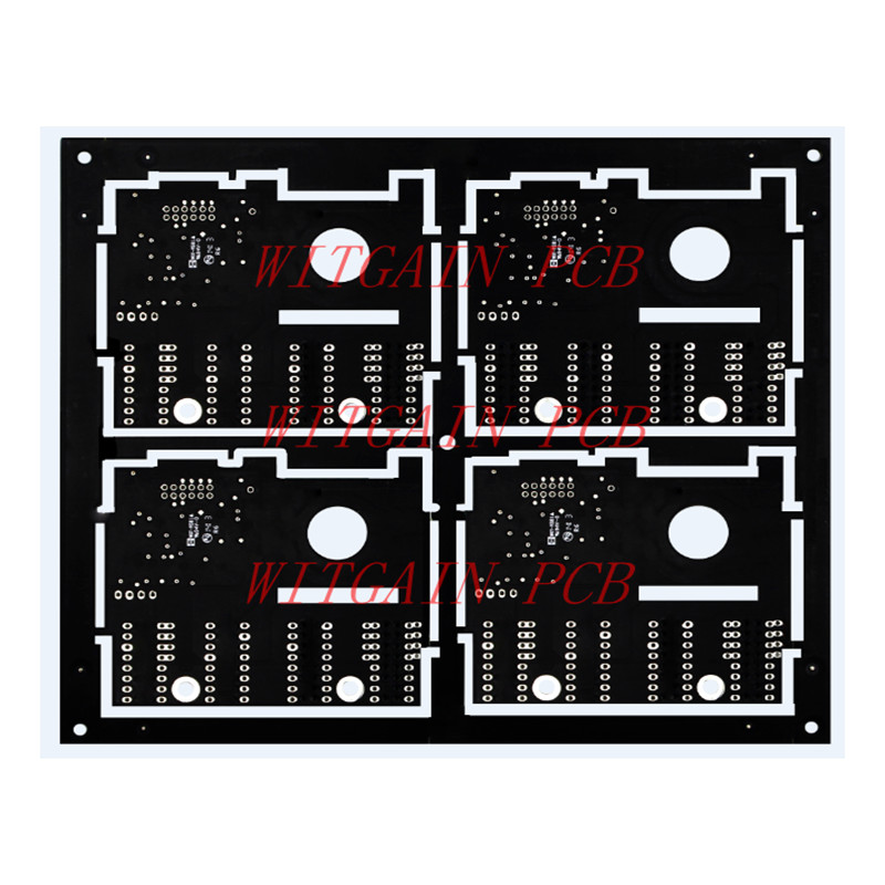
- Design, materials, and process changes require documented approval from both LNPW purchasing and LNPW engineering. 13 . PWB is not panelized.
- There shall be no feature-to-feature spacing less than what is shown in the table below, even if the features are electrically common [i.e., on the same net]. Any clearance present in the gerber data must be present in the fabricated board, subject to workmanship tolerances for the requested class of construction. Starting copper weight Minimum design spacing
(ounces) line-line/pad-pad
================= ==================
0.5 5/5
5 15/17
- MATERIAL: FR-4 Grade, Mid Tg, Non-Dicy [FILLED Phenolic],
500 hr Anti-CAF: Taiwan Union TU-622, Taiwan Union TU-668, and Iteq IT-158. Non-phenolic or Dicy material is not allowed.
All other materials must be approved in advance by LNPW. Once a design is qualified, no changes to material or construction can be made without LNPW approval.
Packaging: Enclose a maximum of 10 panels in individually vacuum-sealed packages.