


| Place of Origin: | China |
|---|---|
| Brand Name: | WITGAIN PCB |
| Certification: | UL |
| Model Number: | PCB0030 |
| Minimum Order Quantity: | 1 pcs/lot |
| Price: | negotiable |
| Packaging Details: | Vacuum bubble bag packaging |
| Delivery Time: | 20 days |
| Payment Terms: | T/T |
| Supply Ability: | 100k pcs/month |
| No Of Layers:: | 4 Layer | Material:: | FR4 TG>150 |
|---|---|---|---|
| Solder Mask Colour:: | Black Solder Mask | PCB Thickness:: | 1.6 MM |
| Surface Technics:: | ENIG | Min Lind Space&Width:: | 3.5/3.5 Mil |
| High Light: | Black Solder Mask 4 Layer PCB,3.5 mil 4 Layer PCB,enig finish pcb |
||
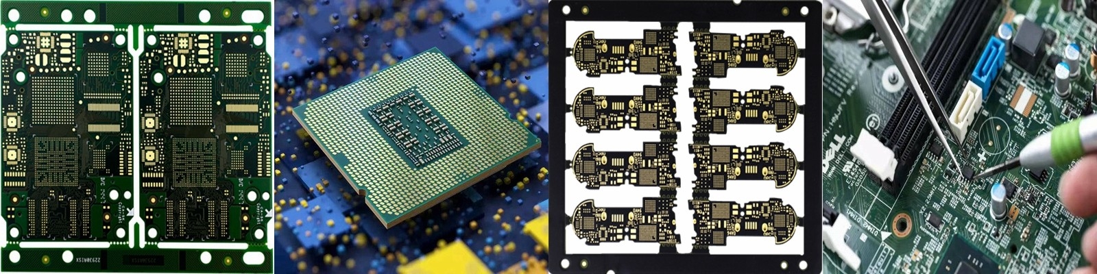
4 Layer PCB 1.6 MM Thickness 1 OZ Copper Black Solder Mask
1 4 Layer Printed Circuit Board PCB .
2 Immersion Gold treatment, gold thickness 1u'.
3 FR4 substrate material, tg150 degree.
4 Min line space and width 3.5/3.5mil.
5 Copper thickness is 1 oz on each layer, 35 um on each layer.
6 Black solder mask and white silkscreen.
7 ROHS, MSDS, SGS, UL, ISO9001&ISO14001 Certificated
| Our Product Categories | ||
| Material Kinds | Layer Counts | Treatments |
| FR4 | Single Layer | HASL Lead Free |
| CEM-1 | 2 Layer/Double Layer | OSP |
| CEM-3 | 4 Layer | Immersion Gold/ENIG |
| Aluminum Substrate | 6 Layer | Hard Gold Plating |
| Iron Substrate | 8 Layer | Immersion Silver |
| PTFE | 10 Layer | Immersion Tin |
| PI Polymide | 12 Layer | Gold fingers |
| AL2O3 Ceramic Substrate | 14 Layer | Heavy copper up to 8OZ |
| Rogers, Isola high frequency materials | 16 Layer | Half plating holes |
| Halogen free | 18 Layer | HDI Laser drilling |
| Copper based | 20 Layer | Selective immersion gold |
| 22 Layer | immersion gold +OSP | |
| 24 Layer | Resin filled in vias | |
Q1: What is a 4-Layer PCB Stackup?
A1: A 4-layer PCB Stackup is a multilayer PCB that consists of multiple layers of copper and insulating materials stacked one above the other. For maximum efficiency and minimum losses and EMI, it is important to plan the right stack up of layers before starting the fabrication process. 4-layer PCB is the most common stack-up arrangement used in modern electronics.
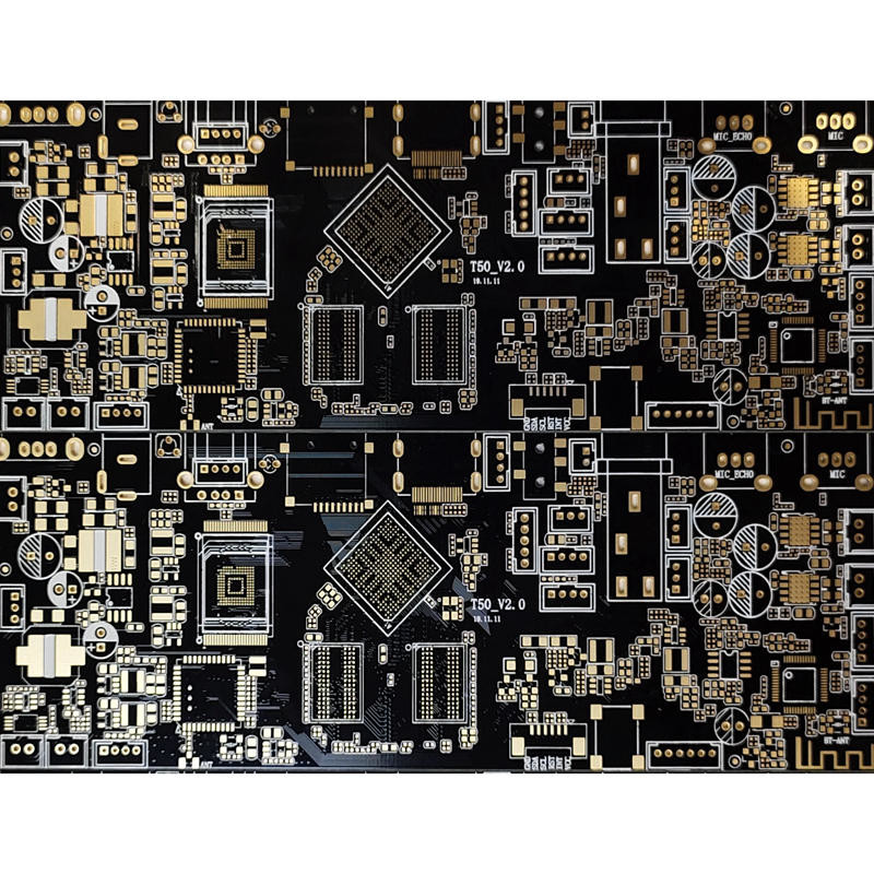
A 4-layer PCB stack up consists of top and bottom layers, a core (copper-clad layer), and an insulating layer also called prepreg made of a dielectric material like glass fiber/weave cloth. The top and bottom layers are made of copper foils, which are then laminated and etched to create slots for mounting the components. The core layer is made up of prepreg sandwiched between two copper foils. These top and bottom layers, core layer, and prepreg are bound together in such a way that no air is trapped between them.![]()
As mentioned in the previous paragraph, the 4-layer PCB comprises the top and bottom layers, prepreg and a core layer. Now, the top and bottom layers, made of copper foils are used as signal planes. After lamination, the desired slots are etched for the placement of components and vias, which are electroplated holes connecting different planes in the PCB. The top side of the core is used as a ground plane, while the bottom side is used as a power plane. To reduce EMI and crosstalk, it is advisable to place the ground plane above the power plane. This will help in the reduction of overlapping and interference of the magnetic fields created by the signal and the current planes. The ground plane also helps in routing the return current and dissipation of heat.
![]()


