


| Place of Origin: | China |
|---|---|
| Brand Name: | WITGAIN PCB |
| Certification: | UL |
| Model Number: | PCB00041 |
| Minimum Order Quantity: | 1 pcs/lot |
| Price: | negotiable |
| Packaging Details: | Vacuum bubble bag packaging |
| Delivery Time: | 20 days |
| Payment Terms: | T/T |
| Supply Ability: | 100k pcs/month |
| No Of Layers:: | 8 Layer | Material:: | FR4 TG150 |
|---|---|---|---|
| PCB Thickness: | 1.6 MM | Solder Mask Colour:: | Blue Solder Mask |
| Surface Technics:: | ENIG 1U' | Copper Thickness: | 1/H/H/H/H/H/H/1 OZ |
| High Light: | 1.6 MM Thickness 8 Layer PCB,UL 8 Layer PCB,ENIG SMT Circuit Board |
||
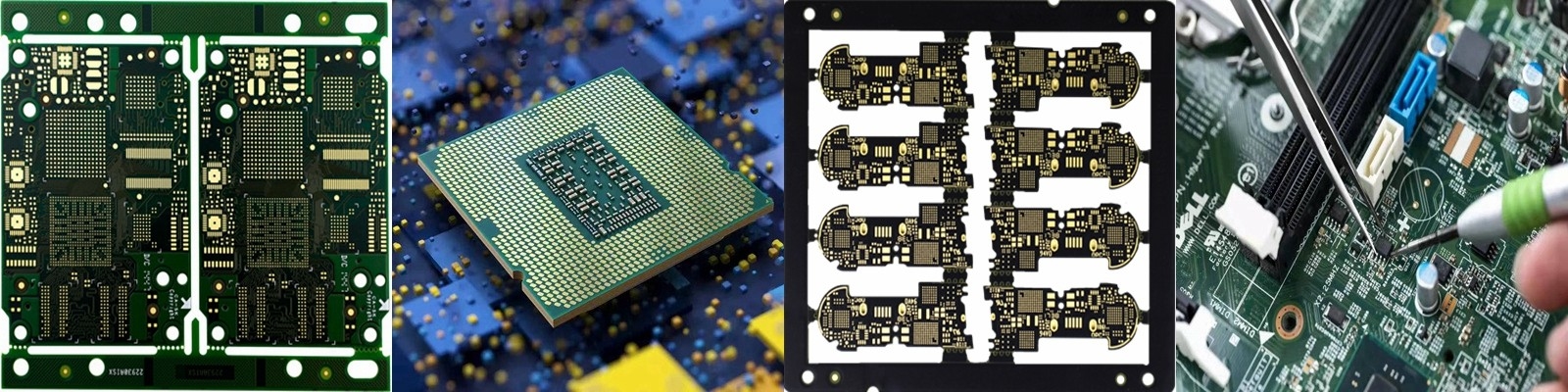
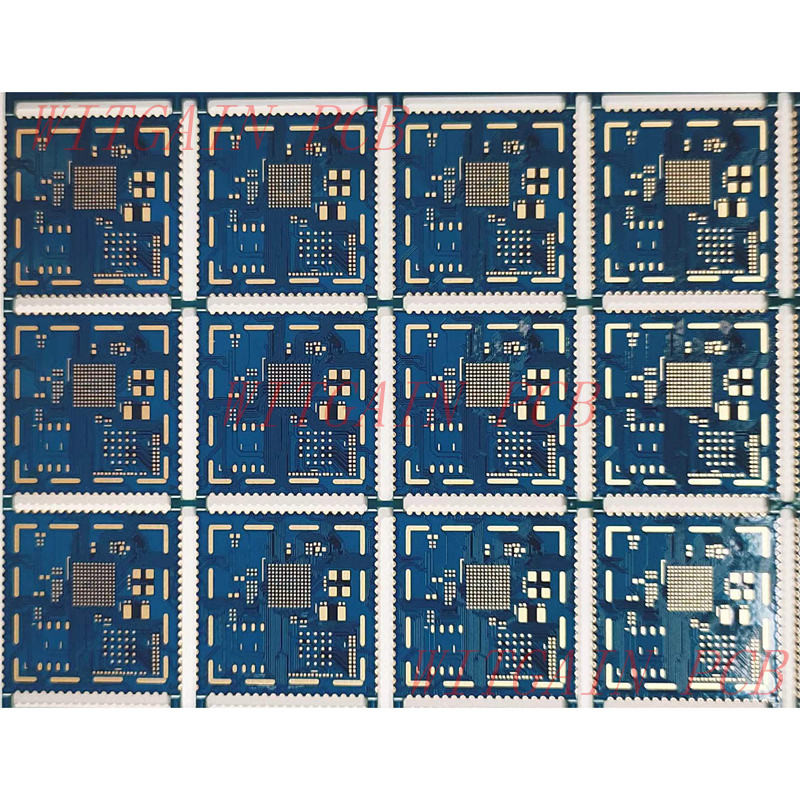
8 Layer PCB Used In GPS Module Blue Solder Mask ENIG
Main Features:
1 8 Layer Printed Circuit Board with very high relability.
2 PCB drawing size is 118.8mm*115mm/12pcs
3 Copper thickness is 35 um on each layer
4 FR4 substrate material ,TG150 degree.
5 Surface treatment is immersion gold.
6 Gold thickness is 1U'.
7 Finished board thickness is 1.6mm.
8 Gerber file or PCB file should be offered by customer before production.
Our Capabilities:
| NO | Item | Capability |
| 1 | Layer Count | 1-24 Layers |
| 2 | Board Thickness | 0.1mm-6.0mm |
| 3 | Finished Board Max Size | 700mm*800mm |
| 4 | Finished Board Thickness Tolerance | +/-10% +/-0.1(<1.0mm) |
| 5 | Warp | <0.7% |
| 6 | Major CCL Brand | KB/NanYa/ITEQ/ShengYi/Rogers Etc |
| 7 | Material Type | FR4,CEM-1,CEM-3,Aluminum,Copper, Ceramic, PI, PET |
| 8 | Drill Hole Diameter | 0.1mm-6.5mm |
| 9 | Out Layer Copper Thickness | 1/2OZ-8OZ |
| 10 | Inner Layer Copper Thickness | 1/3OZ-6OZ |
| 11 | Aspect Ratio | 10:1 |
| 12 | PTH Hole Tolerance | +/-3mil |
| 13 | NPTH Hole Tolerance | +/-1mil |
| 14 | Copper Thickness of PTH Wall | >10mil(25um) |
| 15 | Line Width And Space | 2/2mil |
| 16 | Min Solder Mask Bridge | 2.5mil |
| 17 | Solder Mask Alignment Tolerance | +/-2mil |
| 18 | Dimension Tolerance | +/-4mil |
| 19 | Max Gold Thickness | 200u'(0.2mil) |
| 20 | Thermal Shock | 288℃, 10s, 3 times |
| 21 | Impedance Control | +/-10% |
| 22 | Test Capability | PAD Size min 0.1mm |
| 23 | Min BGA | 7mil |
| 24 | Surface Treatment | OSP, ENIG,HASL, Plating Gold, Carbon Oil,Peelable Mask etc |
FAQ:
Q1:What is PCB Grid Testing or Bed of Nails Testing?
A1: Grid testing or Bed of Nails testing is a process used to check the performance of components mounted on a PCB board. This test uses a frame/fixture that contains various pins inserted into an epoxy phenolic glass cloth laminated sheet (G-10) in order to access all the PCB test points. These pins act as sensors which are aligned to make contact with the test points on the PCB board and are also connected with a measuring unit through wires. The position of the pins is designed and customized for each PCB based on the components or points on the board that need to be tested.
![]()
A grid testing machine has three building blocks - a fixture, a bed of nails and software, to control the overall functionality of the machine. It usually has two cameras which are placed on the top and bottom of the machine in order to scan the whole board.
Advantages of PCB Grid Testing:
Limitations of PCB Grid Testing:
This type of testing is called In-Circuit Testing. Another test process used for In-Circuit testing is Flying Probe Testing.


