

| Place of Origin: | China |
|---|---|
| Brand Name: | WITGAIN PCB |
| Certification: | UL |
| Model Number: | Heavy gold PCB0001 |
| Minimum Order Quantity: | 1 pcs/lot |
| Price: | negotiable |
| Packaging Details: | Vacuum bubble bag packaging |
| Delivery Time: | 20 days |
| Payment Terms: | T/T |
| Supply Ability: | 100k pcs/month |
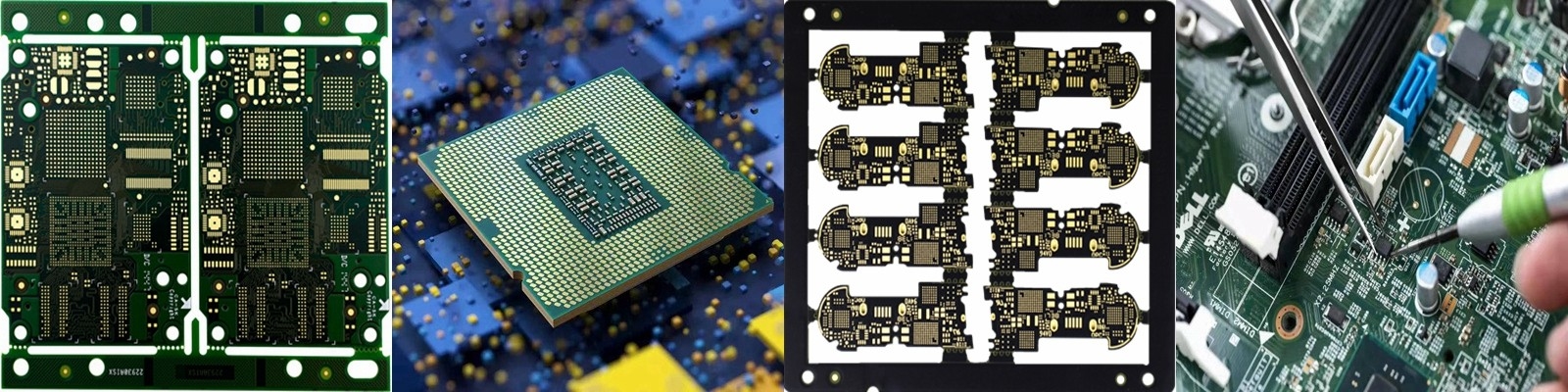
| Product Name: | Gold Finger PCB | Place Of Origin:: | Guangdong China |
|---|---|---|---|
| Material:: | FR4 TG>170 | No Of Layers:: | 2 Layer |
| Solder Mask Colour:: | Black | Surface Technics:: | ENIG+Hard Gold Plating |
| Min Lind Space&Width:: | 5/5mil | OEM: | Yes |
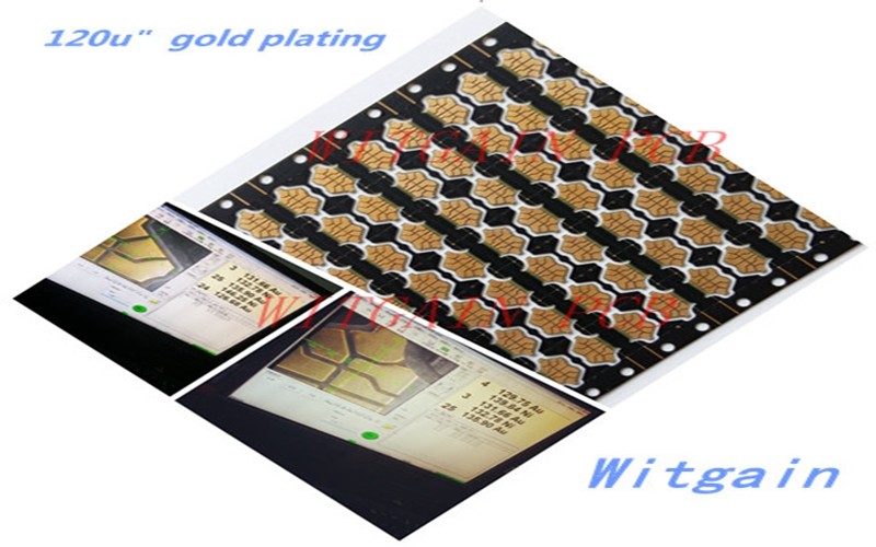
| High Light: | 120u Gold Finger PCB,Gold Finger PCB Circuit Board,PCB Hard Gold Plating |
||
Hard Gold Plating Printed Circuit Board Super Thick Gold Thickness 120u'
1 Super heavy gold on pad, gold thickness is 120u'.
2 Resin filled in vias, all vias plated shut.
3 Top side surface treatment is hard gold plating.
4 Bottom side surface treatment is immersion gold.
5 Black solder mask and white silkscreen.
6 Finished board thickness is 1.0mm.
![]()
Q1: What is the trade term?
A1: EX WORK, FCA SHENZHEN, FOB SHENZHEN, FOB HONGKONG
Q2: What is the lead time of your pcb
A2: It depends on pcb qty and pcb layers. Generally, for 2 layer pcb the sample lead time is about 4-5 days, batch order lead time is 10-12 days. For 4 layer pcb, sample lead time is 7-8 days, batch order lead time is 15-18 days. If customer need pcb very urgently, we will expedite the process and ship it earlier than standard lead time.


