


| Place of Origin: | China |
|---|---|
| Brand Name: | WITGAIN PCB |
| Certification: | UL |
| Model Number: | PCB0037 |
| Minimum Order Quantity: | 1 pcs/lot |
| Price: | negotiable |
| Packaging Details: | Vacuum bubble bag packaging |
| Delivery Time: | 20 days |
| Payment Terms: | T/T |
| Supply Ability: | 100k pcs/month |
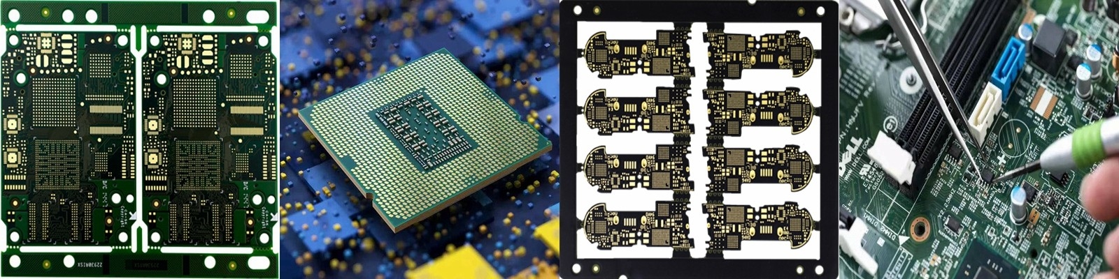
| No Of Layers:: | 6 Layer | Material:: | FR4 TG>150 |
|---|---|---|---|
| PCB Thickness: | 2.0 MM | Solder Mask Colour:: | Black |
| Surface Technics:: | ENIG 1U' | Min Lind Space&Width:: | 3/3 Mil |
| High Light: | 3 Mil LCD Panel PCB,Black Solder Mask LCD Panel PCB,6 Layer Screen Printing Circuit Boards |
||
6 Layer PCB Display Screen Used Black Solder Mask
Printed Circuit Board Features:
Packing Specifications:
1 One vacuum pcb package should not be over 25 panels based on panel size.
2 The vacuum pcb package sealed must be free to tear, hole or any defects that may cause leakage.
3 The pcb package must be suitable to ensure effective vacuum sealing.
4 Every package must have desiccant and humidity indicator card on the inside of vacuum package.
5 Humidity indicator card target less than 10%.
Our history:
![]()
FAQ:
Q1: What is PCB Grid Testing or Bed of Nails Testing?
A1: Grid testing or Bed of Nails testing is a process used to check the performance of components mounted on a PCB board. This test uses a frame/fixture that contains various pins inserted into an epoxy phenolic glass cloth laminated sheet (G-10) in order to access all the PCB test points. These pins act as sensors which are aligned to make contact with the test points on the PCB board and are also connected with a measuring unit through wires. The position of the pins is designed and customized for each PCB based on the components or points on the board that need to be tested.


