


| Place of Origin: | China |
|---|---|
| Brand Name: | WITGAIN PCB |
| Certification: | UL |
| Model Number: | Aluminum PCB00036 |
| Minimum Order Quantity: | 1pcs/lot |
| Price: | negotiable |
| Packaging Details: | Vacuum package in bubble wrap |
| Delivery Time: | 10 days |
| Payment Terms: | T/T |
| Supply Ability: | 100kpcs/Month |
| Layer Count: | 1 Layer | PCB Thickness: | 2.0 MM |
|---|---|---|---|
| CU Thickness: | 1 OZ | Application: | LED Light |
| Lead Time: | 15 Days | Solder Mask: | White Solder Mask |
| High Light: | 2.0MM Single Layer PCB,2W/MK Single Layer PCB,Aluminum Substrate Printed Circuit Boards |
||
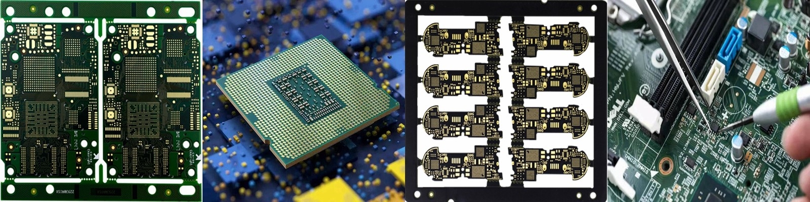
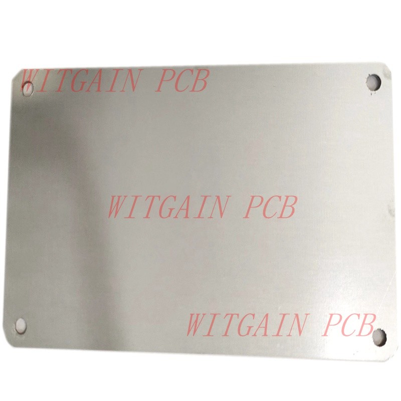
2 W/MK Conductivity Aluminum Substrate Single Layer PCB Used In Led
Specifications:
1 All dimensions are in MM.
2 Fabricate per IPC-6012A Class2.
3 Materials:
3.1 Dielectric: Aluminum
3.2 Min Tg: 150DEG
3.3 Copper: As per stack up
3.4 UL Rating: 94V0 Minimum
4 Surface finish: ENIG 1U
5 Solder mask material should meet all requirement of the IPC-SM-840E and shall be green in color and applied over bare copper. Vendor may edit solder mask and paste mask as needed.
6 Editing of existing copper layers shall require customer approval.
7 Silkscreen legend to be applied per layer stackup using white non-conductitive epoxy ink.
8 100% continuity testing using database netlist shall be performed.Vendor to identify test passed in secondary side.
9 Vendor to mark date code and logo in legend secondary side.
10 Bow and twist shall not exceed 1.0% of longest side.
11 Vendor to provide panel drawing for customer approval before production
PCB report have to include the following information:
1 Measurement: outline dimension, pcb thickness, plating thickness, actual hole size dimension, copper thickness, hole wall copper thickness, solder mask thickness, track and space width, warp and twist percentage;
2 Test and inspection: electrical test result, solder ability test result, visual inspection test result, micro section pcb with resin;
3 Other: date code, quantity etc.
FQA:
Q1: What are PCB Pads?
A1:

A pad on a PCB is an exposed region of metal that allows the soldering of the component leads onto printed circuit boards. These pads are then connected to traces on the board to form a circuit. When no components are soldered on to a PCB, a visible PCB pad footprint can be seen on the board (see figure above).
There are two types of PCB pads:
Through Hole Pads: Pads used to mount through-hole components are known as Through Hole Pads.

They are further differentiated into two types.
a.) Plated Through Hole (PTH) pads:

PTH refers to a pad where the hole wall will be plated with copper or solder or any other material which will have protective plating. The hole plating is done by using electrolysis. This plating provides an electrical connection between the different layers in a board.
b.) Non-Plated Through Hole (NPTH) pads:

NPTH is a pad without any kind of plating in its hole. NPTH pads have holes that are void of any traces of copper which is done to prevent any electric shorts between copper layers and components that will be placed. It is primarily used for single-sided boards where the component can be soldered on the top or the bottom depending on design specifications.
Surface Mount Pads:
Pads used to mount surface mount components are known as surface mount pads. They can be rectangular, round, or square in shape. They are denoted with distinctive pad numbers which are useful for identification purposes during component placement.


