


| Place of Origin: | China |
|---|---|
| Brand Name: | WITGAIN PCB |
| Certification: | UL |
| Model Number: | SSDPCB00013 |
| Minimum Order Quantity: | 1pcs/lot |
| Price: | negotiable |
| Packaging Details: | Vacuum package in bubble wrap |
| Delivery Time: | 15 working days |
| Payment Terms: | T/T |
| Supply Ability: | 1kkpcs/month |
| Layer Count: | 1 Layer | Material: | Copper Substrate |
|---|---|---|---|
| Board Thickness: | 1.8MM | Surface Treatment: | ENIG 1U' |
| Special Feature: | Thermoelectric Separation | Application: | LED |
| High Light: | ENIG Copper Substrate PCB,1.8mm Copper Substrate PCB,1.8mm ENIG PCB |
||
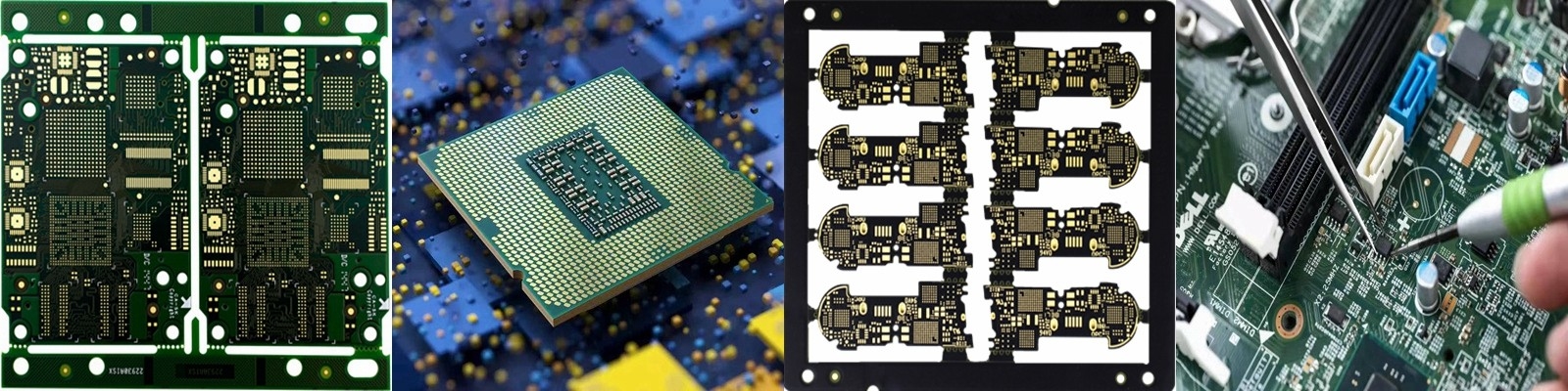
ENIG Copper Substrate PCB High Power LED Thermoelectric Separation
Hign Power LED Thermoelectric Separation Copper Substrate 1 Layer ENIG Printed Circuit Board PCB
PCB Specifications:
Part NO: LEDPCB00001
Layer Count: 1 Layer Printed Circuit Board
Finished Board Thickness: 1.8mm
Copper Thickness: 1
Material: Copper Substrate
Application Area: Hign Power LED
Special Feature: Thermoelectric Separation
Surface Treatment: ENIG
Our Product Categories:
1 FR4 substrate PCB : 2 Layer Printed Circuit Board, 4 Layer PCB, 6 Layer PCB, 8 Layer PCB, 10 Layer PCB, 12 Layer PCB, 14 Layer PCB, 16 Layer PCB, 18 Layer PCB, 20 Layer PCB, 22 Layer PCB, 24 Layer PCB, HDI PCB, High frequency PCB.
2 Aluminum Substrate pcb: 1 Layer Aluminum PCB, 2 Layer Aluminum PCB, 4 Layer Aluminum PCB.
3 Flexible PCB: 1 Layer FPC, 2 Layer FPC, 4 Layer FPC, 6 Layer FPC
4 Rigid-Flex PCB: 2 Layer Rigid-Flex PCB, 4 Layer Rigid-Flex PCB, 6 Layer Rigid-Flex pcb, 8 Layer Rigid-Flex PCB, 10 Layer Rigid-Flex pcb
5 Ceramic substrate pcb: single Layer Ceramic pcb, 2 layer ceramic pcb
FAQ:
Q:What is PCB pads?
A:
A pad on a PCB is an exposed region of metal that allows the soldering of the component leads onto printed circuit boards. These pads are then connected to traces on the board to form a circuit. When no components are soldered on to a PCB, a visible PCB pad footprint can be seen on the board (see figure above).
There are two types of PCB pads:
Through Hole Pads: Pads used to mount through-hole components are known as Through Hole Pads.

They are further differentiated into two types.
a.) Plated Through Hole (PTH) pads:

PTH refers to a pad where the hole wall will be plated with copper or solder or any other material which will have protective plating. The hole plating is done by using electrolysis. This plating provides an electrical connection between the different layers in a board.
b.) Non-Plated Through Hole (NPTH) pads:

NPTH is a pad without any kind of plating in its hole. NPTH pads have holes that are void of any traces of copper which is done to prevent any electric shorts between copper layers and components that will be placed. It is primarily used for single-sided boards where the component can be soldered on the top or the bottom depending on design specifications.
Surface Mount Pads:
Pads used to mount surface mount components are known as surface mount pads. They can be rectangular, round, or square in shape. They are denoted with distinctive pad numbers which are useful for identification purposes during component placement.


