


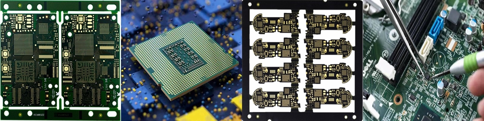


PCBs continue to evolve to enhance their performance, connectivity, compactness, durability, etc. One of the ways they have developed is to include edge or side plating. It is a simple metallization process that gives immense benefits. We will look at PCB edge plating to explain how you can design and build this technical feature into your circuit board. Let's get started.
What is PCB Edge Plating?
PCB edge plating refers to the copper plating or metallization of the sides of a circuit board. And it can be on at least one board edge. These metalized outer edges enhance the board's rigidity to reduce equipment failure, especially on tiny boards, such as Bluetooth and WiFi modules.
A LAN module chip with edge plating on a small section
Also, this metal edging creates a strong connection through the circuit board and has a surface finish that provides an electrical connection. Electroless Nickel Immersion Gold (ENIG) is the preferred surface finish due to its durability and smooth, even finish.
Variations of Edge Plating
The metalized edges can take any of the following four forms.
Wraparound Edge Plating
Wraparound plating involves routing the metalized edge along the sides after drilling. The routing process exposes the PCB sidewall to electroless base copper plating for simultaneous application when applied to the drilled holes.
This base layer creates a conductive surface on which you can place a thicker, more durable copper layer via electroplating (for better adhesion).
An illustration of the copper electroplating process
Castellated Edge Plating (Board Edge PTH)
With castellated edges, the plating does not cover the entire board edge. Instead, it plates holes drilled on the perimeter and extends to the perimeter edge for routing.
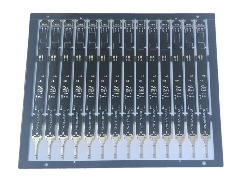
A Bluetooth module with castellated edge plating on two sides
Therefore, this plating type is best for boards requiring peripheral connections. And the peripheral devices can be slaves or modules that augment the main board's performance.
Copper Up-To-Board Edge
This edge plating type maintains a minimum distance between the copper features and the PCB edge. The space can be either of the following.
- 0.45mm on all layers with V-scoring
- 0.25mm on outer layers and 0.4mm on inner layers with break-routing
Only use the copper-to-board edge distance where slight copper damages won't interfere with the board's performance. And the tracks should not be within this distance.
Round Edge Plating
Round edge plating involves metalizing the side from top to bottom. It establishes solid grounds for metal casing or shielding purposes. The production process for this edge plating type involves milling followed by thru-hole plating.
An NVMe M2 SSD PCB with edge plating on the upper side
It is impossible to do 100% continuous metallization around the sides because you must hold the board in the production panel when processing. So there must be gaps for route tabs. And selective chemical nickel-gold is the recommended surface finish for this type.
How To Design An Edge-Plated PCB
Define the plated copper area using overlapping copper in the design/layout file. This extra deposition of copper could be copper pads, surfaces, or traces.
The minimum overlap should be 0.5mm, and the connected copper definition should be 0.3mm on the linked layer sitting on the substrate. So the minimum width of this copper surface should be 0.8mm.
An engineer designing a printed circuit board
On non-connected layers, the copper layer on the board should be at least 0.8mm away from the edge/outer contour. Therefore, the minimum gap from the inner trace to the edge copper layer defined as the connected copper should be 0.5mm.
Metalized Edge Plating Process
This process requires only four steps in the following order.
- Drilling
- Milling metal slot
- Cleaning to get rid of dirt
- Electroless copper plating
The outer contours must undergo milling before thru-hole plating because edge metallization occurs in this fabrication step. And the next step after copper deposition is applying the surface finish.
A PCB in the production process
But these two issues can arise when fabricating the metal edges.
- Copper peeling: Electroless plating over a large substrate area can lead to the copper layer peeling due to minimal adhesion strength. Therefore, you should roughen the surface using proprietary means, such as chemicals. This roughened surface will create a higher copper bond strength when you do direct metallization.
- Burrs: Edge plating can create burrs from the concluding machining process, especially on castellation holes. You can apply a proprietary process flow with minimal modifications to polish the burrs to the feature's edges.
Fabrication Notes
- If the inner edge pad connects to the board's wires, it will create a short circuit.
- A gold pad's antenna position that is too large will affect signal transmission or soldering.
- You can cover the metalized edges with a solder mask layer.
- Design the stamp hole at the edging groove and handle it in the second drilling process.
- All-round edge metallization is impossible on the outer edges through the individual PCB fabrication process as a panel (large volume production). You cannot metalize the small panel bridge locations. However, it is possible on a single board or prototype.
Benefits of PCB Edge Plating
- Enhanced current conduction: Improving the current-carrying capability enhances the board's reliability and quality. Also, the right conduction level is ideal for components to operate as required. And it can protect vulnerable edge connections, as well.
- Signal integrity: Edge plating enhances signal integrity by preventing interference from getting to the internal electrical pulse transmission.
- Thermal distribution: Since the plated edges are metallic, they create an additional cooling surface area for dissipating heat to the surrounding air. As modern PCBs pack more components onto a tinier surface area, these metal surfaces increase the board's reliability, especially if the parts are heat-sensitive.
A mini wireless Bluetooth module for mobile devices
- Better EMC/EMI performance: The metalized edges allow stray currents to escape, preventing sporadic electric and magnetic field generation.
- Improves electromagnetic compatibility: Edge plating enhances electromagnetic compatibility in multilayer boards.
- Prevents electrostatic damage: Electrostatic charges can hit sensitive components when handling the board, but these metal surfaces help absorb them.
PCB Edge Plating Applications
- Edge soldering for better fabrication
- Board-to-board connections
- Increase current carrying capacity
- Enhance connectivity into metal casings (housing connection)
- To enhance EMC performance
Wrap Up
To conclude, PCB edge plating is a simple addition process, but it requires specialized equipment and skilled fabricators to carry out the process with precision. At OurPCB, we have the equipment, trained engineers, and experience to fabricate metalized edge PCBs for your project. Contact us today to get a free quote for your PCB edge plating designs.