


| Place of Origin: | China |
|---|---|
| Brand Name: | WITGAIN PCB |
| Certification: | UL |
| Model Number: | Half hole PCB0009 |
| Minimum Order Quantity: | 1 pcs/lot |
| Price: | negotiable |
| Packaging Details: | Vacuum bubble bag packaging |
| Delivery Time: | 20 days |
| Payment Terms: | T/T |
| Supply Ability: | 100k pcs/month |
| PCB Kind: | HDI PCB | Material:: | FR4 S1000-2 |
|---|---|---|---|
| No Of Layers:: | 4 Layer | PCB Thickness:: | 0.8 MM |
| Surface Technics:: | Immersion Gold | Min Lind Space&Width:: | 3.5/3.5 Mil |
| High Light: | 4 Layer PCB Castellated Holes,PCB Castellated Holes 0.8 MM,HDI Immersion Hard Gold Plating PCB |
||
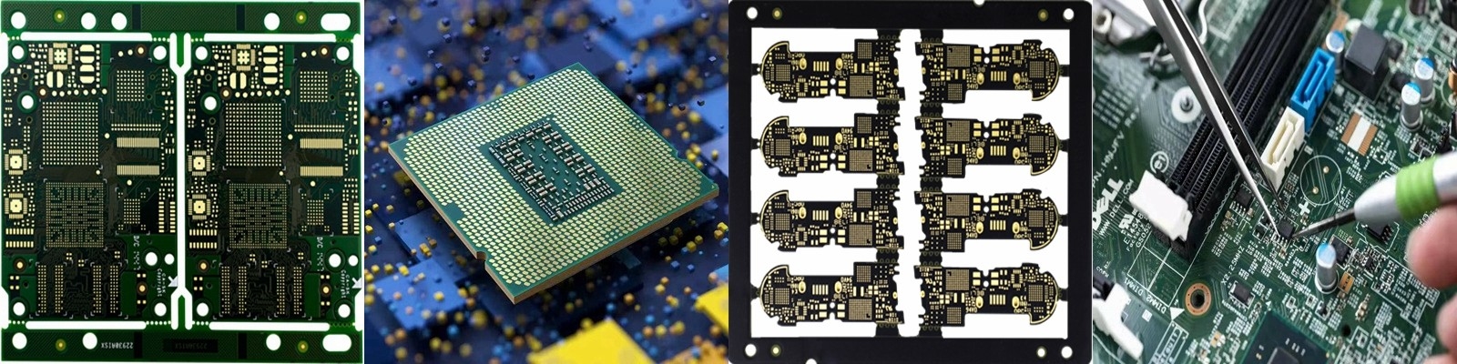
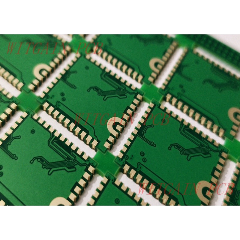
4 Layer PCB Half Hole 0.8 MM Thickness Immersion Gold HDI PCB
Board Info:
1 Part NO: Half hole PCB0009
2 Layer Count: 4 Layer PCB
3 Finished Board Thickness: 0.8 MM tolerance is +/-0.1MM
4 Solder Mask: Green
5 Min Lind Space&Width: 3.5/3.5 mil
6 Application Area: Blue-tooth Module
7 Drillings: L1-L2 0.1MM Laser drilling, L3-L4 0.1MM Laser Drilling, L1-L4 0.2MM Mechanical Drilling
8 BGA Size: 0.2MM, Laser drilling on BGA PAD and plated flat
Packing Specifications:
1 One vacuum pcb package should not be over 25 panels based on panel size.
2 The vacuum pcb package sealed must be free to tear, hole or any defects that may cause leakage.
3 The pcb package must be suitable to ensure effective vacuum sealing.
4 Every package must have desiccant and humidity indicator card on the inside of vacuum package.
5 Humidity indicator card target less than 10%.
FAQ:
Q1: What is an Annular Ring?
A1: A via is created by drilling a hole through a copper pad etched on each layer of a PCB. An Annular Ring is the area between the edge of the drilled via and the copper pad associated with that hole. The greater the width of an annular ring, the greater the copper connection around the drilled via will be.
![]()
In a multilayer PCB, traces are routed from one layer to another layer with the help of vias. These vias are the holes drilled through copper pads on the surface of the PCB. The amount of copper left around the via on both top and bottom sides of the PCB is called the annular ring.
![]()
Mathematically, an annular ring is the difference between the diameter of the hole and diameter of the pad divided by 2. For instance, if the diameter of the pad is 24 mils and the diameter of the hole is 12 mils then the width of the annular ring is [(24-12)/2] = 6 mils
![]()
Calculation of the width of an annular ring plays an important role at the time of PCB manufacturing. If the width of the annular ring is not enough then the hole could touch the boundaries of the pad, this condition is called ‘Tangency’. In the extreme situation, the hole could be outside the boundary of the pad which is termed as ‘Breakout’. Both these situations should be avoided during the process of PCB fabrication.
![]()


