


| Place of Origin: | China |
|---|---|
| Brand Name: | WITGAIN PCB |
| Certification: | UL |
| Model Number: | PCB00312 |
| Minimum Order Quantity: | 1 pcs/lot |
| Price: | negotiable |
| Packaging Details: | Vacuum bubble bag packaging |
| Delivery Time: | 20 days |
| Payment Terms: | T/T |
| Supply Ability: | 100k pcs/month |
| No Of Layers: | 4 Layer | Material: | FR4 TG>170 |
|---|---|---|---|
| Solder Mask Colour: | Green Solder Mask | PCB Thickness: | 1.0 MM |
| Surface Technics: | ENIG 1U' | Min Lind Space&Width: | 4/4 Mil |
| High Light: | 4 Layer Immersion Gold PCB,1.0MM Immersion Gold PCB,Immersion Gold 4 Layer PCB |
||
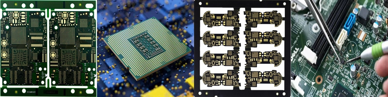
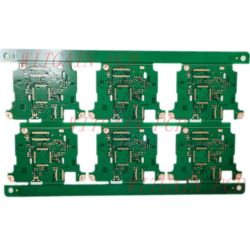
4 Layer PCB Immersion Gold Treatment 1.0 MM Board Thickness Green Mask
1 4 Layer Printed Circuit Board PCB .
2 Immersion Gold treatment, gold thickness 1u'.
3 FR4 substrate material, tg170 degree.
4 Min line space and width 4/4 mil.
5 Copper thickness is 1 oz on each layer, 35 um on each layer.
6 Green solder mask and white silkscreen.
7 ROHS, MSDS, SGS, UL, ISO9001&ISO14001 Certificated
8 Application Area: Earphones
| Our Product Categories | ||
| Material Kinds | Layer Counts | Treatments |
| FR4 | Single Layer | HASL Lead Free |
| CEM-1 | 2 Layer/Double Layer | OSP |
| CEM-3 | 4 Layer | Immersion Gold/ENIG |
| Aluminum Substrate | 6 Layer | Hard Gold Plating |
| Iron Substrate | 8 Layer | Immersion Silver |
| PTFE | 10 Layer | Immersion Tin |
| PI Polymide | 12 Layer | Gold fingers |
| AL2O3 Ceramic Substrate | 14 Layer | Heavy copper up to 8OZ |
| Rogers, Isola high frequency materials | 16 Layer | Half plating holes |
| Halogen free | 18 Layer | HDI Laser drilling |
| Copper based | 20 Layer | Selective immersion gold |
| 22 Layer | immersion gold +OSP | |
| 24 Layer | Resin filled in vias | |
Q1: Preventing Plating and Solder Voids
A1: While manufacturing printed circuit boards or PCBs, we focus our attention to the handling of tools and processes. This helps us avoid many quality issues like cold joints, brittle joints, and voids. As their name suggests, voids are empty spaces. Ideally, voids have no place in PCBs. The presence of voids in a PCB confirms that somewhere along the manufacturing activity, the process did not add enough of a certain material. Not addressing the void issue properly and in time may lead to in increase in the fall-off-rates.
For the understanding of our customers and to highlight the problems that void formation creates, we will explain the nature of voids and how we avoid them. PCBs generally suffer from two types of voids during the manufacturing process. And we will highlight the measures we take to avoid creating them.

PCB Voids
PCB voids occur wherever there are non-plated areas in the circuit board. These could be within solder joints, or within barrels of holes, or within the wall of a drilled and plated through hole. The presence of voids can disrupt electrical connections, leading to malfunctioning of the board.
PCB voids are generally of two types—solder voids and plating voids. Solder voids occur when not using adequate amounts of solder paste, or when the solder paste has air pockets that have not escaped as the paste heats up. Plating voids can occur during deposition of electroless copper when the plating does not entirely cover the inner wall of the through hole. Although in stray cases it may be possible to repair the board manually, the presence of voids is a serious issue that can render the PCB inoperable, and leave the manufacturer without any choice but to scrap the board.
Solder Voids
An empty space within a solder joint constitutes a solder void. This issue can arise from many factors. One of the major factors is the low preheat temperature in the reflow or wave soldering oven, which prevents the solvents in the flux from vaporizing totally. Other factors that can cause voids in solder are oxidization of solder paste, high levels of flux, or use of low-quality solder paste. The design of some PCBs can also contribute to being prone to voiding.
Preventing Solder Voids
Solder voids are easy to prevent. This is best done by increasing preheat temperature, slowing down travel time through the oven, avoiding use of outdated or low-quality solder paste, or modifying the stencil of the board. All these steps can be effective in mitigating the risk of solder voids.
Plating Voids
Plating voids typically occur because of the drilling process and the preparation of the through hole. Ideally, the drill bit must leave a smooth wall in a through hole it drills. Using a dull drill bit may leave the inner surface of the wall uneven, rough, and not clean throughout. As copper enters the hole during the plating process, it may cover the contaminants and debris inside the hole. When the debris dislodges later, it may leave a bare non-plated spot. This may cause a void, as the copper does not adhere totally to the surface wall of the hole. The uneven surface of the hole may also prevent copper from covering every crevice of rough spot, leaving behind a non-plated spot.
Plated through holes in a PCB connect conductive circuits on one side of a layer to another circuit on an adjacent layer. These electrical connections help in carrying through power and signals to all parts of the board. Whenever there is an interruption, such as due to the presence of a void, the disruption of electrical signals and power may cause a malfunction in the circuit and the board.
If there are a number of such interruptions, and the inspection is unable to locate all of them, the board may have to be scrapped. Moreover, there is no guarantee that more voids will not show up later on, disrupting the operation of the board in the field. Therefore, preventing voids is a key objective when fabricating PCBs.
Preventing Plating Voids
Avoiding plating voids is best achieved through the use of sharp and well-formed drill bits. When drill bits are sharp, they create a clean hole that has no roughness and is clean throughout the hole. Copper has no problem covering the smooth wall and forming a barrel without any discontinuity or voids.
When drilling, even with sharp and well-formed drill bits, the speed of drilling is an important issue. If the drilling rate is fast, the drill bit may shatter the PCB material as it advances. This can lead to rough and uneven surfaces inside the hole wall that is difficult to plate.
During the drilling process, it is necessary to sharpen drill-bits depending on drill speed, bit count records, and drill feeds. Every drilled hole requires a cleaning procedure, and proper racking. When plating, monitoring and controlling the plating bath agitation may also help to reduce and eliminate plating voids, by removing entrapped air bubbles.
Conclusion
If boards need scrapping because of the presence of voids in them, the manufacturing process can become prohibitively expensive. However, as our experience at Witgain PCB Ltd shows, some extra attention to detail and some precaution can prevent most void formations in PCBs.
We have established detailed drilling and cleaning procedures. We also conduct extensive and thorough testing to reduce void formation and ensure the quality of the boards we produce. Furthermore, we also provide manufacturing design reviews between us and customers to help save on costs while ensuring a smoother production process for our boards.


