


| Place of Origin: | China |
|---|---|
| Brand Name: | WITGAIN PCB |
| Certification: | UL |
| Model Number: | HDIPCB0026 |
| Minimum Order Quantity: | 1pcs/lot |
| Price: | negotiable |
| Packaging Details: | vacuum package in bubble wrap |
| Delivery Time: | 25 days |
| Payment Terms: | T/T |
| Supply Ability: | 100kpcs/Month |
| Solder Mask: | Green Solder Mask | Layer Count: | 10 Layer |
|---|---|---|---|
| Board Thickness: | 1.2MM | Min Hole: | 0.1MM |
| Copper Thickness: | H/H/H/H/H/H/H/H/H/H | Surface Treatment: | Immersion Gold 2U' |
| Size: | 800mm*60mm | BGA Size: | 8 MIL |
| High Light: | HDI Printed Circuit Board Assembly,1.2MM Printed Circuit Board Assembly,Immersion Gold prototype circuit board |
||
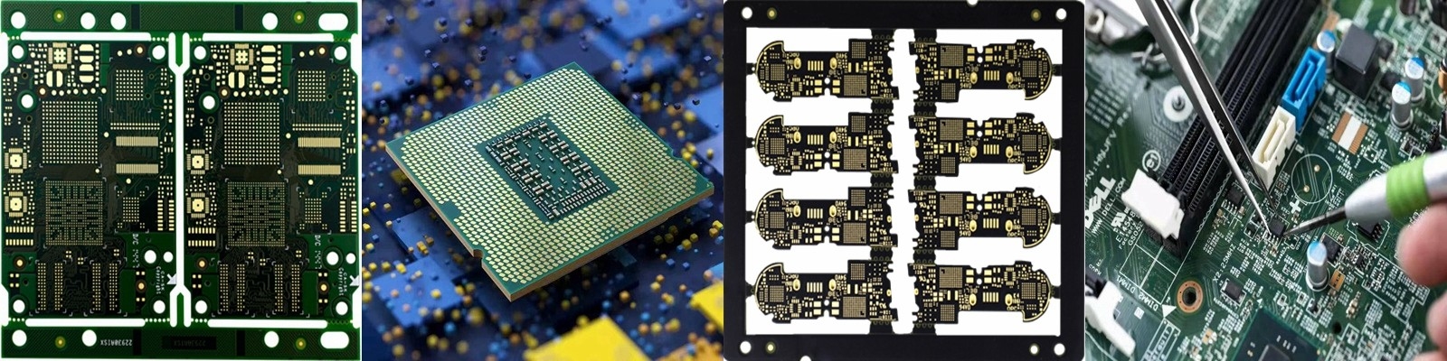
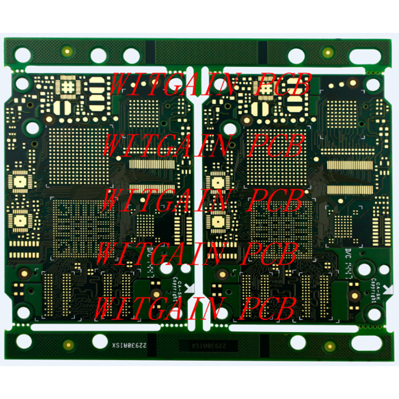
HDI PCB 10 Layer 1.2MM Thickness Immersion Gold 2U' FR4 Substrate
PCB Specifications:
1 Part NO: HDIPCB0026
2 Layer Count: 10 Layer HDI PCB
3 Finished Board Thickness: 1.2MM
4 Hole Structure: L1-L2 0.1MM, L2-L3 0.1MM, L3-L4 0.1MM, L4-L5 0.1MM, L5-L6 0.1MM, L6-L7 0.1MM,
L7-L8 0.1MM, L8-L9 0.1MM, L1-L10 0.15MM
5 Min Lind Space&Width: 2.5/2.5mil
6 Copper Thickness: H/H/H/H/H/H/H/H/H/H
7 Application Area: Consumer Porducts
Our production applications:
1 Consumer electronic products: SSD, TWS earphones, headsets,computer devices, portable power supplies, bluetooth modules, gps modules, wifi modules, smart keys for cars, intelligent locks, floor mopping robots, zigbee, etc.
2 Industrial control:main boards in machines, industrial robots, servo motors etc.
3 Automotive: BMS main boards, automotive radar etc.
4 Power supplies: UPS, industrial power supply, frequency power supply.
5 Medical: medical equipment, medical equipment power supply.
6 Communication products: 5G base station, routers, satellites, antennas.
FAQ:
Q1: What is the Thermal Resistance of a PCB?
A1: PCB makes the dispersion of heat easier. This is basically the inverse of thermal conductivity. The thermal resistance of a PCB can be calculated by evaluating all the layers of the board and the heat parameters of the material.
To find the total thermal resistance for your board, you must include all layers of the board and the associated heat parameters for the type of material through which heat will flow.
[Formula]
R_theta = absolute thermal resistance (K/W) across the thickness of the sample
Delta x = thickness (m) of the sample (measured on a path parallel to the heat flow)
k = thermal conductivity (W/(K·m)) of the sample
A = cross-sectional area (m2) perpendicular to the path of heat flow
In addition to the thermal resistance of the board. The Thermal resistance of Vias must also be calculated. This usually depends on the copper trance, the laminate and the substrate and their respective thermal resistivities.
How can you reduce the Thermal Resistance of a PCB?
Thermal resistance can be reduced by increasing the thickness of the copper traces.
Another method to decrease the thermal resistance is to place copper pads below the hot components. The high thermal conductivity of copper provides a low resistance path for the dispersion of heat. These pads can be connected to an internal ground plane through vias, which have good thermal conductivity and thus help move heat away from the component.
Using Heat Sinks can help lower the thermal resistivity of the board.


